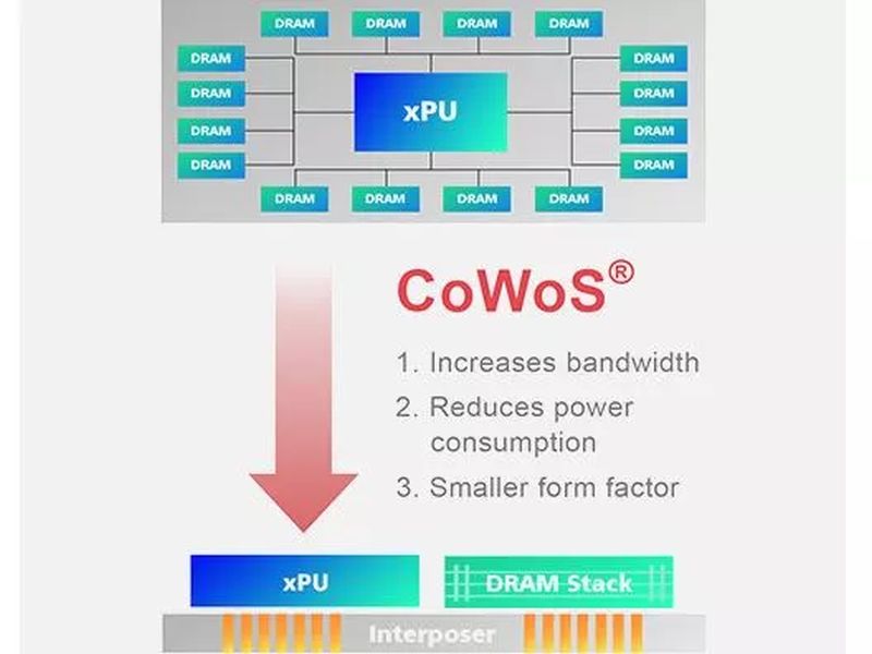
In addition to the current process, TSMC had also reportedly shared some details about the future beyond 3nm, something that the company is calling 3DFabric technology. According to Tom’s Hardware, the concept of 3DFabric focuses on advanced packaging technologies and as such, 3D packaging technologies were determined to be the next step after 3nm. To be clear, this wouldn’t be TSMC’s first foray into the development and manufacturing 3D packaging techniques; to date, the company has used technologies such as Chip-on-Wafer-on-Substrate (CoWoS), Integrated Fan Out (InFO-R), Chip on Wafer (COW), and Wafer-on-Wafer (WoW). All of which are now part of its new 3DFabric family.
As to what TSMC intends to develop with its new 3DFabric technology, we’re probably in for a long wait. After all, the technology was announced to take place after 3nm development, meaning that we may only see some semblance of the technology sometime after the year 2022. Getting back to the 5nm, TSMC says that it’s 5nm N5 processor will offer full-node scaling compared to the current 7nm process node, as well as up to 15% more performance. Either at the same power as the 7nm die lithography or at 30% less power. Further, TSMC says that the defect density learning curve for 5nm would be significantly faster than the 7nm process and that could result in higher yield rates. (Source: Tom’s Hardware, AnandTech)